← 100 Kirby Coloring Pages: Free Printable PDF for Fans Kirby coloring sword printable pages How to Draw a Star Properly: Perfect Shapes Every Time Super easy how to draw a star tutorial for kids →
If you are looking for Schematic Drawing Programs For Pcb Layout you've came to the right page. We have 25 Images about Schematic Drawing Programs For Pcb Layout like PCB Drawings: 5 Drafting Standards | ALLPCB, The Basics of PCB Design W/ CAD | PCB Train and also PCB Assembly Drawing. Here it is:
Schematic Drawing Programs For Pcb Layout
 guidemanualtheek.z21.web.core.windows.net
How To Design A PCB Layout - Circuit Basics
 www.circuitbasics.com
pcb layout circuits electronics campbell posted
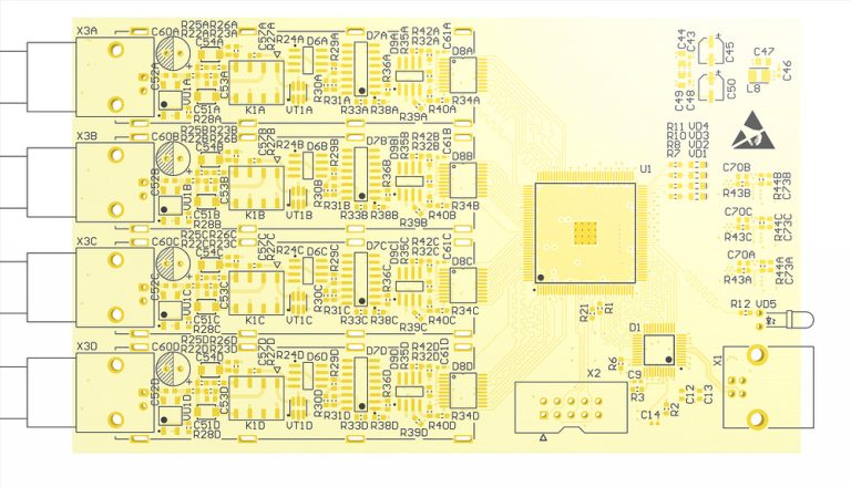
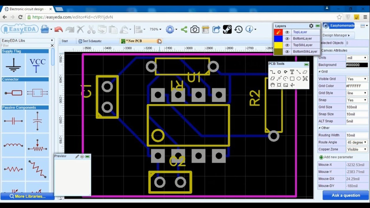
Altium Pcb Layout Tutorial Laying Out Your Pcb In Altium Designer
 pcbways.pages.dev
Conveying Your PCB Design Intent With PCBA Drawing Creation In
 resources.altium.com
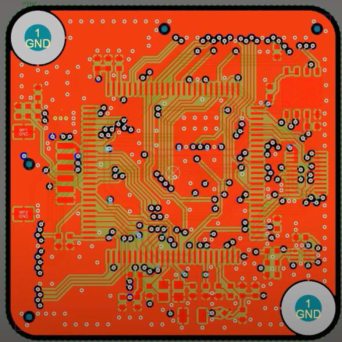
A Detailed Guide To PCB Layout Design |Qtech Technology Co. Ltd
 qtech-us.com
Printed Circuit Board | Bicheng PCB
 www.bicheng-enterprise.com
pcb panelization specify
PCBA Drawing: What Are The Basic Requirements For Assembly Drawing?
 www.ourpcb.com
4-Layer PCB Design In KiCad 5: Quick Thoughts | Paul Bupe, Jr
 paulbupejr.com
pcb kicad layer quick
How To Design Your Own PCB – From Basic Layout Tips – PCB HERO
 www.pcb-hero.com
PCB Drawings: 5 Drafting Standards | ALLPCB
 www.allpcb.com
pcb drawings standards drafting allpcb figure
How To Design A Pcb Layout Pcb Designs - Bank2home.com
 www.bank2home.com
PCB Assembly Drawing: Designing For Seamless Fabrication - MorePCB
 morepcb.com
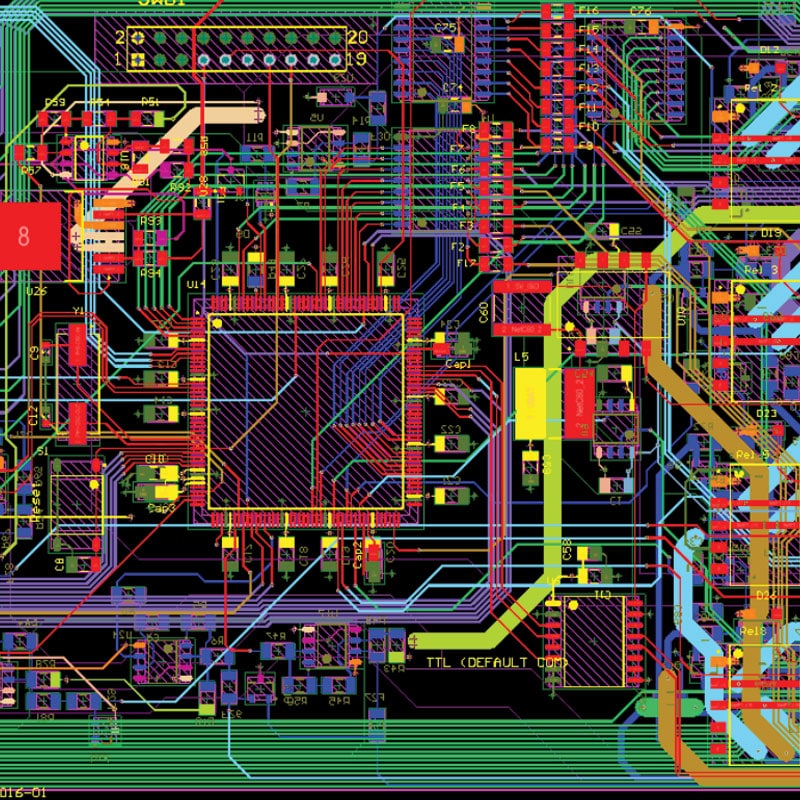
PCB Layout Design By Siemens | PADS Professional | Cadlog
 www.cadlog.com
pcb mentor pads xpedition vx designers environment 2d getintopc circuit siemens descrição detalhada
PCB Layout Design By Siemens | PADS Professional | Cadlog
 www.cadlog.com
pcb pads rf construction siemens try
A Comprehensive Guide To Understanding PCB Assembly Drawing Requirements
 www.europepcb.com
Design Your Pcb Layouts By Dinusharg | Fiverr
 www.fiverr.com
The Basics Of PCB Design W/ CAD | PCB Train
 www.pcbtrain.co.uk
pcb layout cad design schematic review pcbs do designing basics improve efficiency lay file e2e ti capture allpcb shutterstock
Drawing A Pcb To Precise Dimensions - Layout - KiCad.info Forums
 forum.kicad.info
pcb drawing kicad precise
How To Read A PCB Fabrication Drawing
 www.optimumdesign.com
Power Pcb Design, Elctrical Printed Circuit Board Design And Layout For
 www.venture-mfg.com
pcb layout power design high supply board speed tips guide designing autodesk courtesy allpcb funender layer
Circuit Board Manufacturing Design Process | Product Creation Studio
 www.productcreationstudio.com
Pcb Design Guidelines Book - Design Talk
 design.udlvirtual.edu.pe
Electronic Schematic Capture And Simulation Program Schemati
 diagramstadijisdq.z14.web.core.windows.net
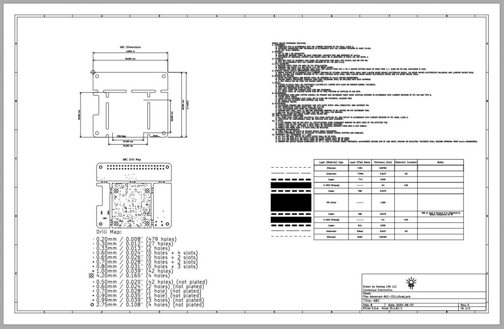
PCB Assembly Drawing
 pcbinsider.com
Make Sure To Consider These Factors When Creating A PCB Layout - Blog
 www.pcbunlimited.com
pcb layout blog
Pcb layout blog. Altium pcb layout tutorial laying out your pcb in altium designer. How to read a pcb fabrication drawing